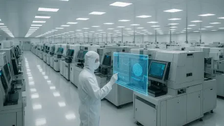

Applied Materials has introduced specialized systems to accelerate the complex stack and deposition steps required for advanced 3D packaging. This development highlights a broader structural transformation within the semiconductor manufacturing industry, which is rapidly shifting from traditional, labor-intensive trial-and-error methodologies to sophisticated, data-driven automated decision-support systems. At the heart of this evolution lies the recipe copilot software market, a specialized sector encompassing advanced platforms designed to assist process engineers in the development, optimization, and validation of the precise instructions governing equipment interactions with silicon wafers. These digital assistants are becoming indispensable for critical fabrication steps such as lithography, etching, and deposition, where the margin for error has effectively vanished. As the global semiconductor landscape becomes more competitive and technically demanding, the emergence of these software tools represents a direct response to the increasing complexity of modern chip architectures. By leveraging high-fidelity data and advanced algorithms, recipe copilots enable a level of precision that was previously unattainable through manual tuning alone.
Navigating the Complexity of Next-Generation Silicon Nodes
As the semiconductor industry moves toward 2nm processes and beyond, the manufacturing environment has reached a point where traditional human-centric engineering is no longer sufficient to maintain high yields. The “process window,” defined as the specific range of parameters within which a chip can be successfully manufactured, has shrunk to nearly microscopic margins. Every adjustment to gas flow, plasma density, or exposure time carries significant risks of creating defects that could render an entire batch of wafers useless. This extreme sensitivity necessitates a shift toward software-driven optimization that can account for thousands of variables simultaneously. Recipe copilot software fills this gap by utilizing Bayesian optimization and reinforcement learning to analyze tool traces and metrology data in real time. This capability allows engineers to identify the “sweet spot” of manufacturing parameters much faster than they could through physical experimentation, effectively widening the usable process window and ensuring that the transition to smaller nodes remains economically viable for large-scale production.
The technological leap required for 2nm nodes also introduces new challenges in material science and structural integrity that demand constant recipe refinement. In a modern fabrication plant, or fab, the volume of data generated by a single tool during a single shift is staggering. Without an intelligent copilot to filter this noise and provide actionable insights, engineers often find themselves overwhelmed by information while lacking clear direction. Recipe copilot platforms provide this clarity by offering recommendations that shorten experiment cycles and significantly improve final yield. These systems do not just store data; they transform process learning into a governed and repeatable workflow that survives the turnover of individual engineering staff. By institutionalizing this knowledge, semiconductor companies can protect their intellectual property while accelerating the pace of innovation. This transition is not merely a matter of convenience but a fundamental requirement for any firm aiming to lead in the production of high-performance computing components and advanced mobile processors.
Economic Projections: Growth and Absolute Opportunity
The economic outlook for the recipe copilot software market is characterized by aggressive expansion and high capital commitment from global players. In 2025, the market reached an estimated valuation of USD 43.9 million, and by 2026, this figure is projected to climb to USD 55 million. While these figures represent a niche segment within the broader semiconductor equipment industry, the long-term trajectory suggests a massive scaling of adoption. By 2036, the market is expected to reach a staggering USD 520 million, reflecting a compound annual growth rate of 25.2% over a ten-year period starting from the current year. This growth is underpinned by the absolute opportunity of USD 465 million that will be captured as fabs worldwide modernize their software stacks. The rapid rise in valuation indicates that recipe copilots are moving from experimental “nice-to-have” tools to essential infrastructure for high-volume manufacturing environments where efficiency gains of even a fraction of a percent can translate into millions of dollars in saved costs.
This financial growth is also driven by a fundamental shift in how fabrication engineering teams manage their operational expenditures. Traditional methods of testing a process window required numerous physical experiments, each involving the use of expensive test wafers and valuable tool time. By replacing these physical trials with software-driven simulations and optimization cycles, companies can drastically reduce their research and development costs. In 2026, worldwide fab equipment spending is projected to reach USD 133 billion, and a growing portion of this investment is being allocated to the digital layer that controls the hardware. As the industry scales, the manual management of thousands of unique recipes across multiple product lines becomes a logistical impossibility. Consequently, the demand for intelligent software that turns process intellectual property into a scalable asset is skyrocketing across the global semiconductor ecosystem, from boutique design houses to the largest foundries in the world.
Technological Foundations: Bayesian Optimization and Machine Learning
In 2026, Bayesian optimization is expected to command a dominant 38.0% share of the recipe copilot software market due to its unique efficiency in handling limited and noisy data scenarios. Unlike standard deep learning architectures that require massive datasets to provide accurate predictions, Bayesian engines are designed to provide meaningful direction from just a few samples. In a fabrication environment, where every experimental wafer can cost thousands of dollars, the ability to find an optimal recipe with the fewest number of physical trials is a massive competitive advantage. These optimization engines allow engineers to focus exclusively on the most promising recipe parameters, significantly compressing the time required for the design of experiments. By building a probabilistic model of the process, the software can suggest adjustments that maximize the probability of success while minimizing the risk of tool downtime or wafer breakage, creating a safer environment for experimentation.
Beyond Bayesian methods, the market is seeing a surge in the integration of large language models and reinforcement learning to create a more holistic advisory experience. Large language models are being utilized to query decades of historical fab data, allowing junior engineers to tap into the “tribal knowledge” of the organization through natural language interfaces. Meanwhile, reinforcement learning agents are being developed to suggest autonomous adjustments for tool drift, ensuring that once a recipe is optimized, it stays within the required specifications over thousands of cycles. This multi-layered approach to machine learning ensures that recipe copilots are versatile enough to handle the varied needs of different process steps. Whether it is predicting the chemical vapor deposition rate or optimizing the plasma etch profile, these algorithms are providing the analytical depth necessary to solve the industry’s most persistent engineering bottlenecks without the need for constant human supervision.
The Strategic Role: Digital Twins in Modern Fab Environments
There is a growing consensus among industry leaders that virtual models must precede physical production to ensure operational efficiency in the modern era. In 2025, significant government funding was allocated to establish dedicated research institutes focused on semiconductor digital twins, and these initiatives are now yielding practical results in 2026. A digital twin serves as a high-fidelity virtual replica of a physical tool or process, allowing engineers to explore various process conditions without ever touching a physical wafer. Major semiconductor companies have emphasized that these virtual environments are the primary training grounds for recipe copilot software. By running millions of simulations within a digital twin, the copilot can identify potential points of failure and optimize instructions before a single gram of precursor gas is used. This “virtual-first” strategy ensures that when a recipe is finally deployed to a physical tool, it is already highly refined and ready for high-volume production.
The adoption of digital twin technology also addresses the problem of tool-to-tool variability, which is a significant source of yield loss in large-scale fabs. Even when two machines are of the exact same model, slight differences in internal components or age can lead to different results for the same recipe. Recipe copilot software, integrated with digital twins, can create specific “offsets” for each individual tool, ensuring that the final output remains consistent across the entire production floor. This level of granular control is essential for the manufacturing of high-bandwidth memory and next-generation logic chips, where uniformity is critical for electrical performance. As facilities scale their operations to meet the demand generated by the explosion of generative AI and advanced automotive electronics, the ability to synchronize physical hardware with digital intelligence is becoming the defining characteristic of a world-class manufacturing facility.
Segmenting the Market: Lithography and Process Sensitivity
In 2026, lithography is projected to account for approximately 27.0% of the recipe copilot software market share, making it the most significant application segment. Lithography is widely considered the most sensitive and expensive part of the fabrication process, where even the slightest misalignment or dosage error can have a catastrophic cascading effect on downstream yield. Issues with overlay, dose management, and focus windows require constant monitoring and adjustment, tasks that are perfectly suited for the rapid analytical capabilities of a recipe copilot. By optimizing the instructions for extreme ultraviolet (EUV) and deep ultraviolet (DUV) scanners, these software tools help manufacturers push the boundaries of what is physically possible in terms of circuit density. The precision provided by the copilot ensures that the intricate patterns required for modern transistors are transferred to the wafer with absolute fidelity, reducing the need for costly rework.
Following lithography, the etching and deposition segments are also emerging as major drivers of market growth. These steps require precise control over plasma chemistry, film thickness, and temperature gradients to maintain the integrity of microscopic circuits. As chips become three-dimensional, such as in the case of advanced 3D NAND and gate-all-around (GAA) transistors, the complexity of these recipes increases exponentially. A recipe copilot can analyze the tool sensors during an etch process to detect subtle changes in plasma behavior and recommend immediate adjustments to prevent over-etching or under-etching. This real-time or near-real-time advisory capability is vital for maintaining the structural integrity of high-aspect-ratio features. By providing specialized modules for each of these process steps, software vendors are able to offer tailored solutions that address the specific physical and chemical challenges inherent in different parts of the semiconductor manufacturing flow.
Security and Sovereignty: Preference for On-Premise Solutions
A defining characteristic of the semiconductor industry is its extreme and uncompromising focus on the protection of intellectual property. This culture of secrecy heavily influences how recipe copilot software is deployed across the global ecosystem. Consequently, on-premise deployment is anticipated to capture 51.0% of the market share in 2026, as manufacturers remain deeply reluctant to move their proprietary recipe histories and tool-trace data to the public cloud. The risk of cybersecurity breaches or state-sponsored intellectual property theft is viewed as an existential threat to the competitive advantage of leading chipmakers. On-premise solutions allow for rigorous data governance where sensitive information stays within the physical network and under the direct control of the plant’s security team. This ensures that the specialized knowledge gained through years of process engineering remains a private asset, even as it is enhanced by AI.
Despite the rise of cloud computing in other industries, the semiconductor fab remains a stronghold of localized data processing. Manufacturers often require that the AI models powering their copilots be trained on-site using dedicated hardware, ensuring that no data “leaks” into shared environments. This requirement has led software vendors to develop “edge-ready” versions of their platforms that can run efficiently on local servers without sacrificing performance. Furthermore, on-premise deployment mitigates the risks associated with latency and connectivity, which are critical when software is providing real-time recommendations for high-speed manufacturing tools. By prioritizing secure data silos and localized control, the industry is balancing the need for advanced AI-driven insights with the traditional requirement for absolute operational security, a trend that is expected to persist as geopolitical tensions continue to shape the global technology supply chain.
Regional Dynamics: The Impact of Global Investment and Policy
The United States is expected to record the highest growth rate in the recipe copilot market through 2036, a trend driven by massive domestic investments and strategic research initiatives. Government funding for digital twin technology and advanced packaging has created a fertile environment for software vendors to pilot their most advanced optimization tools. Major domestic plans for DRAM manufacturing and the construction of new logic fabs are further accelerating the need for sophisticated, software-driven process controls that can compensate for a relatively high-cost labor environment. In the U.S. context, recipe copilots are seen as a productivity multiplier, allowing a smaller team of highly skilled engineers to manage a larger fleet of tools effectively. This focus on automation is central to the national strategy of reshoring semiconductor manufacturing and ensuring long-term technological leadership in the face of global competition.
In the Asia-Pacific region, the demand for recipe copilots is driven by different but equally compelling factors. Taiwan remains the world’s leading hub for advanced logic chips, where the move into 2nm volume production necessitates the use of every available tool to shorten learning cycles and maintain yield supremacy. For Taiwanese manufacturers, speed to market is everything, and software that can shave weeks off a qualification cycle is worth its weight in gold. Similarly, South Korea’s memory-heavy economy relies on the optimization of complex 3D NAND stacks, where even a slight recipe drift can be catastrophic for the performance of high-density storage devices. Meanwhile, China is seeing significant growth in its domestic software industry as it seeks to optimize mature nodes through efficiency gains, bypassing some of the limitations imposed by international export controls on advanced hardware. Each region is adopting recipe copilot technology to solve its unique set of manufacturing and geopolitical challenges.
The Competitive Landscape: Giants versus Specialized Providers
The competitive environment for recipe copilot software is a complex mix of established semiconductor equipment giants and agile, specialized software providers. Leaders in materials engineering are increasingly integrating process-control software directly into their proprietary toolsets, offering a seamless experience where the hardware and the “brains” behind it are sold as a single package. These incumbents leverage their deep knowledge of tool physics to create models that are highly accurate from day one. However, this has also opened the door for independent software vendors who offer tool-agnostic platforms. These third-party copilots are particularly attractive to foundries that operate equipment from multiple different suppliers and need a unified software layer to manage recipes across their entire fleet. This tension between integrated and agnostic solutions is driving a wave of innovation that benefits the end-user through more robust and feature-rich options.
For software vendors to succeed in this market, there is an urgent and non-negotiable need to provide “explainability” in their AI models. Semiconductor engineers are notoriously skeptical of “black-box” solutions; they will not adopt a recipe change if they do not understand the underlying physical or chemical logic provided by the software. Consequently, the most successful platforms are those that can demonstrate exactly how a specific suggestion connects to observed wafer results or sensor readings. Platforms must provide visualizations and data correlations that allow a human engineer to validate the software’s reasoning. This push for transparency has led to the development of hybrid models that combine pure machine learning with physical models based on the laws of thermodynamics and fluid dynamics. By bridging the gap between empirical data and scientific theory, software providers are building the trust necessary to move toward more autonomous manufacturing environments.
Future Restraints: Data Silos and Environmental Considerations
Despite the overwhelming positive outlook, the market faces significant hurdles regarding data access and the persistence of organizational silos. Manufacturers are often protective of data not just from external competitors, but also between different customer accounts or internal process modules. Creating a recipe copilot that can learn across these silos without compromising privacy requires sophisticated data isolation and encryption techniques. Furthermore, the speed of software optimization is currently limited by the speed of physical metrology. If a software tool recommends a recipe change, the engineer still needs to wait for the wafer to be processed and measured by an inspection tool to verify the results. Until metrology becomes faster or more integrated into the process tools themselves, the “feedback loop” that the copilot relies on will remain a bottleneck that limits the ultimate speed of innovation.
As recipe models become more complex and digital twin simulations more detailed, the electricity and compute resources required to run these systems are also becoming a point of scrutiny. Modern fabs are already massive consumers of energy, and the addition of high-performance computing clusters to run real-time AI optimization adds to this burden. Sustainability-minded facilities are beginning to evaluate the environmental impact of their digital infrastructure, leading to a demand for more energy-efficient algorithms and specialized hardware accelerators. Balancing the need for advanced AI-generated insights with the rising costs and energy demands of those systems will be a key challenge for the next decade. Success in the market will eventually belong to those who can provide the most intelligence with the lowest computational footprint, ensuring that the drive for manufacturing excellence does not come at an unacceptable environmental or operational cost.
Strategic Imperatives for the Future of Manufacturing
The recipe copilot software market represented a fundamental shift in how the semiconductor industry managed its collective expertise and operational knowledge. By the end of 2025, it became clear that the era of relying solely on the intuition of veteran engineers had passed, replaced by a system where software served as a permanent repository for process learning. This transition was essential for navigating the extreme complexities of the 2nm node and the move toward 3D chip architectures. Manufacturers that successfully integrated these tools saw significant reductions in their development cycles and a marked improvement in their ability to scale new products quickly. The market’s journey toward a half-billion-dollar valuation by 2036 highlighted the critical role of artificial intelligence in bridging the gap between theoretical process models and the messy, high-stakes reality of real-world manufacturing excellence.
Looking ahead, the most critical step for semiconductor leaders is the establishment of a robust data pipeline that can feed these intelligent systems without compromising security. Companies should focus on standardizing their data formats and investing in on-premise high-performance computing to ensure that their recipe copilots have the “fuel” they need to perform. Furthermore, fostering a culture of collaboration between software data scientists and traditional process engineers will be necessary to overcome the skepticism associated with AI-driven recommendations. As the industry moves toward closed-loop automation, the focus will likely shift from simple advisory tools to systems that can autonomously maintain a fab’s health. By prioritizing explainability, security, and integration, the semiconductor ecosystem will ensure that recipe copilot software continues to be a primary driver of the next generation of technological breakthroughs, ultimately defining the winners of the silicon race for the next decade and beyond.